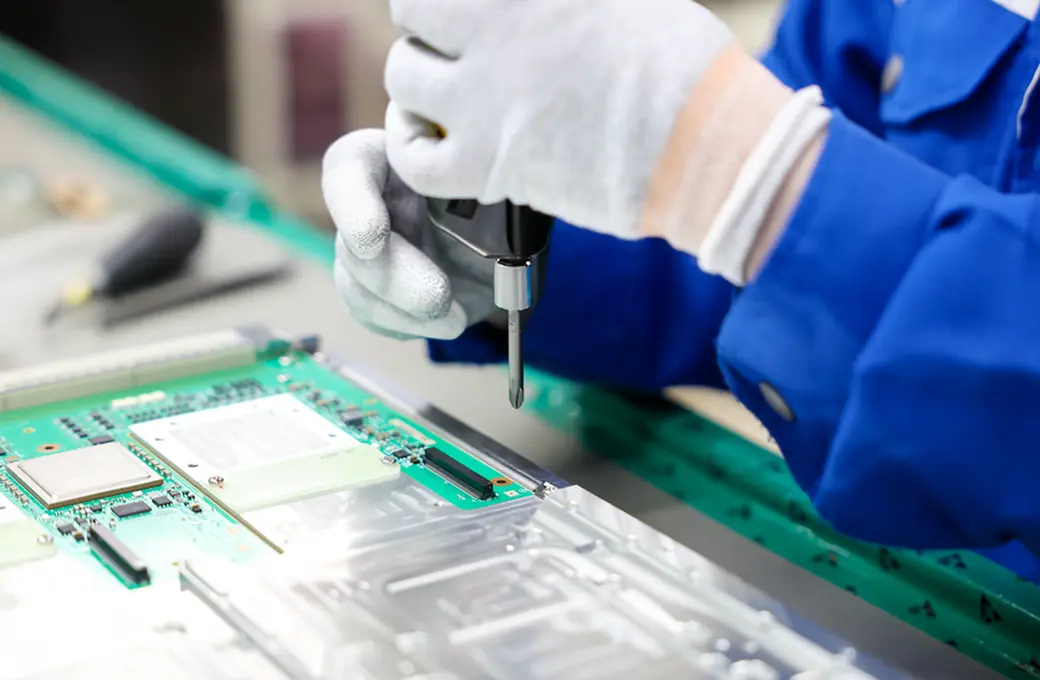
Technical Support from the Development Stage
-
PCB pattern and layout design support
(circuit design, mechanical design, and evaluation) -
Component selection and evaluation services when components are changed
![]()
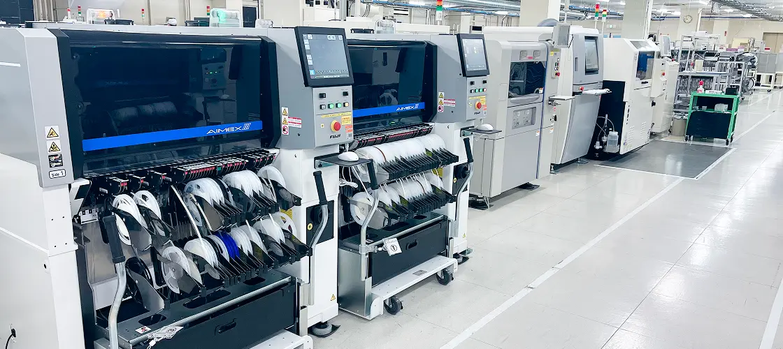
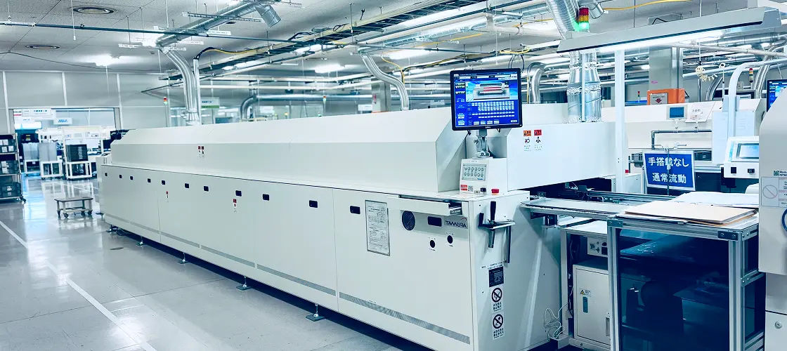
| SMT Lines | 11 lines |
|---|---|
| Maximum PCB Size | LL 510mm × W 460mm |
| Major Equipment (Examples) |
|
The terms described here are used as customary expressions within our company and do not represent official or precise definitions.
CPH (Chip Per Hour)
An abbreviation of “Chip Per Hour,” indicating how many chips a mounting machine can place in one hour. For example, 20,000 cph means the machine can mount 20,000 chips per hour under the manufacturer’s optimal conditions.
EEMS (Electronics Manufacturing Services)
Companies that provide contract manufacturing services for electronic components and devices.
SMT (Surface Mount Technology)
Surface mount technology.
Axial component
Electronic components with leads extending in opposite directions along the same axis. These are generally through-hole components and are not commonly mounted by SMT.
ASSY: Assembly
The process of mounting electronic components onto a printed circuit board.
Underfill
An encapsulating resin used to improve connection reliability of IC packages such as BGA and CSP.
Print pressure
The pressure applied by the squeegee to the metal mask during the solder paste printing process.
Solder Paste Printer
In the SMT industry, a printer refers to a machine that screen-prints solder paste onto the board surface.
Surface treatment
Surface treatment of a PCB to improve solderability by applying finishes such as solder leveling, electrolytic gold plating, electroless gold flash, or heat-resistant pre-flux to the pads before assembly.
Calibration
Adjustment performed to ensure accurate and stable reproduction using image processing.
Teaching
Manually setting and storing component size and related data in the machine.
Crack
Refers to cracks or fractures, such as cracks in solder joints or in the body of components in SMT processes.
Creeping
In soldering, a phenomenon where solder joints gradually deform when a continuous load is applied to the mounted component.
Coplanarity
Flatness or planarity. Coplanarity refers to the uniformity of the lowest points of all terminals or electrodes of a component relative to the mounting surface.
Silk screen print
Printing symbols, circuit identifiers (addresses), model names, lines, etc. on a PCB. White is typically the standard color.
Self-alignment
A phenomenon in which, even if chip components are slightly misaligned during placement, surface tension of the solder during reflow causes the IC to move to the correct position (center of the land) on the PCB pattern.
Chip
Electronic components mounted by a chip mounter, such as chip resistors and chip ceramic capacitors (commonly called “ceramic caps”). Small SMDs are generally referred to as chips.
Chip Mounter / SMD placing machine
A machine used to place SMDs (surface-mount electronic components). Formally called an electronic component placement machine; names such as chip mounter or chip shooter vary by manufacturer.
Modulars placing machine
A type of placement machine that fixes the PCB in a set position and moves the nozzle head to place components.
Radial component
Electronic components with parallel leads extending in the same direction.
Reflow
A process in the SMT line where SMDs are mounted onto a board printed with solder paste and then heated in a reflow oven to melt the paste and form solder joints.
Reflow soldering system
Equipment used for soldering in an SMT line. It can be broadly classified into air reflow and nitrogen reflow systems, with heating methods incorporating manufacturer-specific know-how.
Rotary head type placing machine
A placement machine in which the PCB is fixed on an XY table and moved to specified positions, while multiple placement heads mounted on a rotating drum perform component placement.
CAD (Computer Aided Design)
A computer-based tool that supports design work. Compared to manual design, CAD enables faster and higher-quality work, and most high-layer-count or high-complexity designs have shifted to CAD-based design.
Gerber Data
Includes both circuit and component characteristics such as resistance, capacitance, rated power, and breakdown voltage. This data is essential for creating component libraries, and the importance of unifying Gerber data with component and board libraries has been increasingly recognized.
Bill of Materials / Parts List
A list of components used on a circuit board. It includes reference numbers, part numbers, and attributes. Recently, some schematic editors allow the entire bill of materials to be output at once.
Parts Library
Information for individual components mounted on a circuit board. By unifying circuit symbols and data (component characteristics, part numbers, pin assignments) with footprint data (component shape, dimensions, pin layout, polarity, land pattern), design lead time can be shortened and design errors reduced.
Plotted Drawing
Wiring information output on paper. Used to check routing of power lines and critical patterns, and also used as part of specifications.
Board Library
Defines the standards of a circuit board. It includes board outline, area constraints (mounting area, routing area, height restrictions), layer structure, pre-assigned data (components and routing), grid settings, wiring and hole/land specifications, and solder resist and silkscreen information.
Debug
The process of identifying and correcting defects (bugs) in a program.
PCB (Printed Circuit Board)
Generally refers to a printed circuit board on which electronic components are mounted. In some cases, it is used synonymously with PWB.
V-Cutting
Grooves made along the boundary between boards or between a board and a scrap panel to facilitate separation.
Core Material
Inner-layer material prepared prior to lamination in multilayer boards.
Spot Facing
Machining the board surface to a specified depth. Used to partially expose inner-layer copper foil or to stabilize component positioning during assembly.
Squeegee
A resin tool used to print resist ink or solder paste onto a board. It moves across the screen to press ink or paste through the stencil.
Screen Printing
A printing method in which patterns, resist, or characters are formed on a mesh stencil. Stainless steel screens are commonly used for solder paste printing in assembly.
Solder Resist
An insulating layer that suppresses surface degradation of the board and prevents solder from adhering to unwanted areas. Depending on the process, it may be ink-based, liquid resist, or dry film.
Dent
A surface indentation caused by external pressure. JIS standards define it as damage that does not penetrate the conductor layer.
Copper Foil
Thin copper used in printed circuit boards. There are two types: electrolytic copper foil and rolled copper foil. Electrolytic copper foil is commonly used except for flexible boards.
Pattern Plating
A manufacturing method in which solder or other material is plated onto conductor patterns as an etching resist before etching.
Build-Up Printed Circuit Board
A fabrication method in which insulating and conductive layers are sequentially built up after forming the innermost layer pattern. Its use has expanded due to the demand for higher-density boards.
Footprint
Refers to the land pattern for surface-mount components such as QFPs and SOPs. Also called pads.
Pre-Flux
A chemical coating applied to suppress oxidation of printed circuit boards. Water-soluble and resin types exist, with water-soluble pre-flux becoming common for environmental considerations.
Flexible Printed Circuit (FPC)
A circuit board with conductors formed on a flexible resin substrate. Base materials include polyimide film, polyester film, and glass epoxy, with rolled copper foil used for conductors.
Baking
The process of heating boards under specified temperature and time conditions to remove moisture.
Perforation
A method of making boards easier to separate by applying slit processing and continuous hole drilling along the boundary. Serves the same purpose as V-cutting.
Metal Core Board
Generally refers to a board laminated with aluminum. Due to aluminum’s heat dissipation properties, it is used for high-heat applications such as LED boards.
Work Size
The size required to load a board into the manufacturing line.
ASIC (ASIC:Application Specification Integrated Circuit)
An integrated circuit designed for a specific application.
BGA (Ball Grid Array)
An SMD package in which solder balls are arranged in a grid pattern on the underside of the IC package. Compared to QFPs, BGAs enable higher IC integration and high-density mounting, but visual inspection after assembly is difficult.
COB (Chip On Board)
A mounting method in which a bare chip is directly mounted on a printed circuit board and connected using wire bonding.
CR (Capacitor&Resistor)
Capacitors and resistors.
CSP (Chip Size Package)
A package with the same basic structure as a BGA, but with the package size reduced to be close to that of the bare chip.
DIP (Dual inline Package)
A package in which leads extend from both sides of the package. The leads are bent and inserted into through-holes on the board.
LGA (Land Grid Array)
A type of semiconductor package similar to BGA, but without solder ball bumps on the mounting surface.
MCM (Multi Chip Module)
A module in which multiple semiconductor chips, or a combination of semiconductors and small components, are mounted on a single substrate.
SMD (Surface Mount Device)
Components designed for surface mounting.
SOP (Small Out-line Package)
A package with leads extending from both sides of the package. Unlike DIP, SOP refers to a surface-mount type package.
ELV Directive (End of Life Vehicles)
An EU regulation on vehicle recycling. Similar to the RoHS Directive, it specifies certain hazardous substances.
ICP Mass Spectrometry (ICP-MS)
An analytical method that ionizes atoms in a high-temperature plasma and performs mass analysis in a vacuum environment. It offers higher detection sensitivity than X-ray fluorescence (XRF) analyzers.
ICP Atomic Emission Spectroscopy (ICP-AES)
An analytical method that identifies elements based on the characteristic wavelengths of light emitted by atoms in a high-temperature plasma. Although less sensitive than mass spectrometry, it provides higher sensitivity than XRF analyzers.
MSDS (Material safety data sheet)
Documentation that comprehensively describes the properties of chemical substances and handling precautions. Preparation is required under chemical substance regulations (e.g., PRTR).
Lead-Free (Pb-free)
Refers to solder materials or electronic components that contain no lead, as well as parts and materials that do not use lead.
Red Eye (No Solder)
A phenomenon in which solder does not fully wet the entire land during assembly, leaving exposed copper areas. This defect tends to occur more frequently with lead-free solder due to its lower wettability.
Wicking
A phenomenon in which solder climbs up the leads of surface-mount components during reflow. It is more likely to occur during rapid heating, but can be prevented by sufficient preheating.
Temperature Cycling Test
Also known as a thermal cycling test. An accelerated test involving repeated heating and cooling, used to estimate the service life of printed circuit boards.
Eutectic Solder
Generally refers to solder composed of Sn (62%) and Pb (38%), but also includes alloys whose melting and solidification points are identical. This solder has a eutectic point of 183°C. In contrast, commonly used lead-free solder in Japan (Sn-3.0Ag-0.5Cu) is a non-eutectic alloy.
Creep Properties
A phenomenon in which strain gradually develops over time under load at the solder–substrate joint, eventually leading to fracture. The rate of progression increases at higher temperatures.
Solder
Generally refers to an alloy composed of approximately 63% tin (Sn) and 37% lead (Pb), commonly known as eutectic solder.
Soldering
The process of melting solder to form an alloy layer between component electrodes and the footprint (land) on a printed circuit board.
Solder Ball (Non-wetting)
Ball-shaped solder that forms on the side of a chip, representing one type of assembly defect.
Shrinkage Cavity
A solidification crack that occurs during the solder solidification process. It is not a progressing crack by itself, but larger cavities may become initiation points for cracks due to aging or vibration stress.
Void
Gas bubbles within solder. Voids are commonly observed inside solder balls when mounting BGA or CSP packages, and this tendency is more pronounced in lead-free soldering.
Cold Solder
A condition in which solder is not properly bonded to the component electrode. One type of assembly defect.
Lift-off
A phenomenon in which the solder fillet peels away from the land after flow soldering. It is likely to occur when a low-melting-point alloy layer forms at the interface between the land and the solder.